")
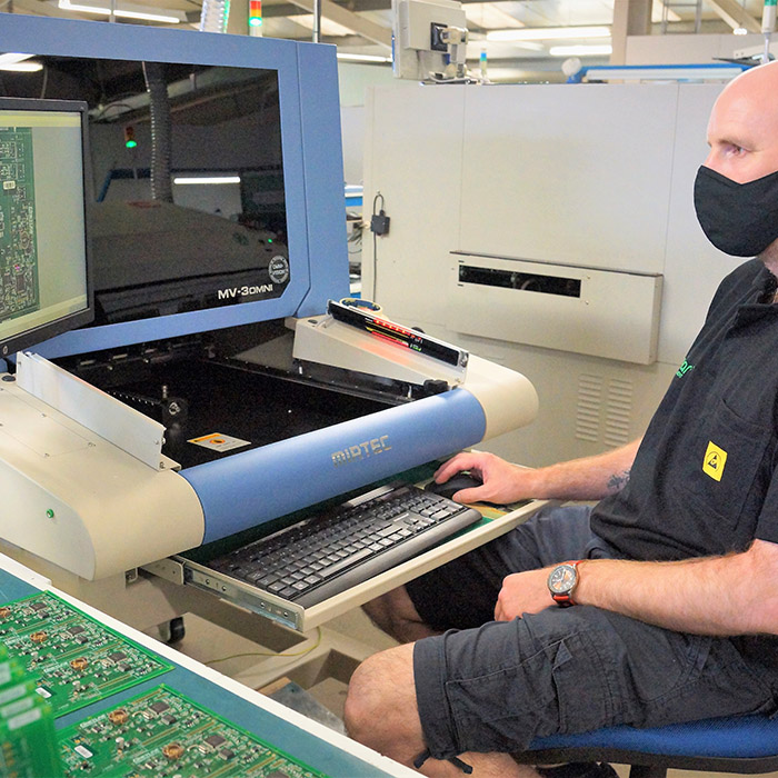
Automated Optical Inspection (AOI)
What is AOI?
Automated Optical Inspection (AOI) is a technique used to ensure the flawless execution of PCB assemblies with unprecedented accuracy. Leveraging advanced optical technologies and sophisticated algorithms, AOI is designed to scrutinize the components on the surface of PCB assemblies with meticulous attention to detail.
Click here to view More Details
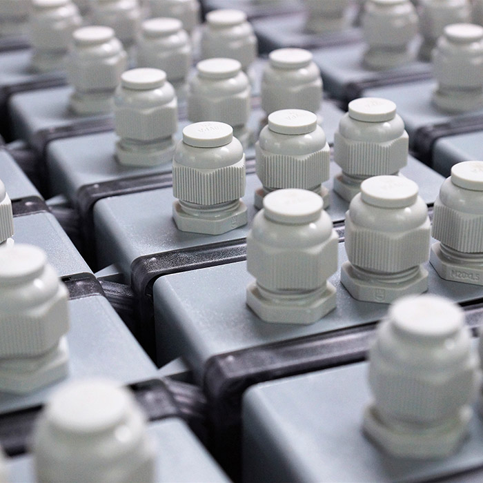

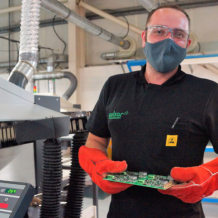
Box Build Assembly
What is Box Build?
Box Build, also known as System Integration or Turnkey Assembly, is the final and crucial phase in PCB manufacturing where the assembled PCB is integrated into a complete electronic system or device. This all-encompassing process involves the assembly of various components such as PCBs, cables, connectors, and mechanical enclosures, resulting in a fully functional and ready-to-use electronic product.
Click here to view More Details

Conformal Coating
What is Conformal Coating?
Conformal coating is a protective, breathable coating of thin polymeric film applied to printed circuit boards. Conformal coating is typically applied at 20-25μm thickness, and designed to protect against moisture and other harsher conditions. Conformal Coating is now considered standard practice in PCB assembly and is applicable across a wide array of different industries.
Click here to view More Details

Encapsulation
What is Encapsulation?
Encapsulation, also known as potting is the process of encasing the printed circuit board (PCB), or parts of it, in a resin. This protective resin serves multiple purposes, including shielding sensitive electronic components from environmental factors, enhancing durability, and improving resistance to mechanical stress.
Click here to view More Details

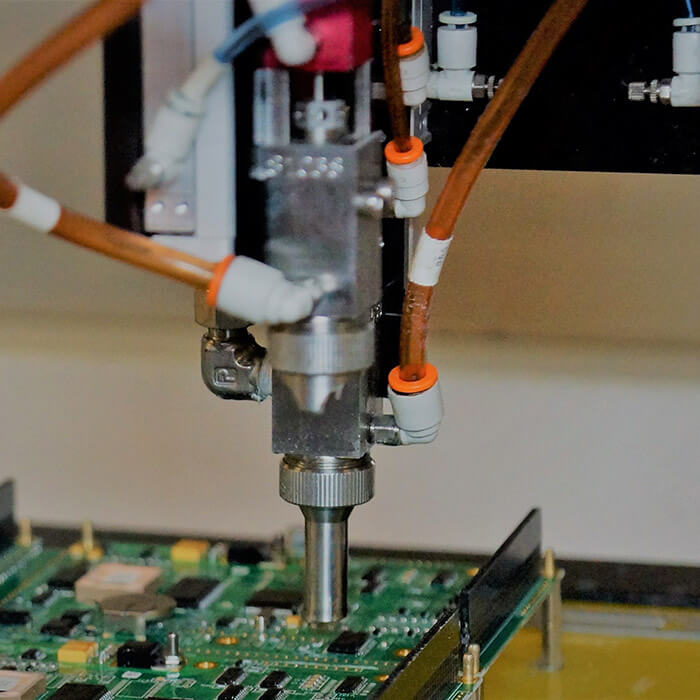
Flow Soldering
What is Flow Soldering?
Flow Soldering, also known as wave soldering, is a crucial step in the PCB (Printed Circuit Board) manufacturing process. It is an automated soldering technique used to efficiently and reliably solder electronic components onto a PCB. This method is particularly suitable for through-hole components, which have leads that pass through holes in the PCB. Throughout the Wave Soldering process, the circuit board is passed over a bath of molten solder, where a pump produces an upwelling of solder that looks like a standing wave. As the circuit board makes contact with this wave, the components become soldered to the board.
Click here to view More Details
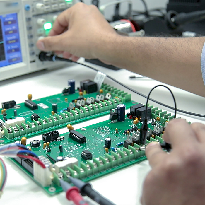

Functional Testing
What is Functional Testing?
At the heart of every electronic device lies a Printed Circuit Board (PCB), a complex interconnection of components that forms the backbone of functionality. Ensuring the reliability and functionality of these PCBs is paramount in today's rapidly evolving technological landscape. That's where the Functional Test in PCB Manufacturing becomes crucial.
Click here to view More Details

Printed Circuit Board Cleaning
What is Printed Circuit Board Cleaning?
The primary goal when cleaning PCB assemblies is to remove resin and flux residues. Although a 'no-clean' process is suitable for most industrial applications a further cleaning process is required for military, medical and aerospace.
Click here to view More Details

PCB Rework
What is PCB Rework?
PCB Rework is the meticulous process of repairing and modifying printed circuit boards that have undergone manufacturing or assembly issues. Whether it's correcting errors, replacing components, or enhancing existing designs, PCB rework is the key to salvaging valuable electronic assembles and ensuring they meet the highest standards of functionality and reliability.
Click here to view More Details
")
Surface Mount Technology (SMT)
What is Surface Mount Technology (SMT)?
Surface Mount Technology revolutionises PCB assembly by placing components directly onto the surface of the PCB, as opposed to through-hole technology that inserts components into drilled holes. SMT enhances the manufacturing process by optimizing space, reducing weight, and facilitating automated assembly techniques.
Click here to view More Details
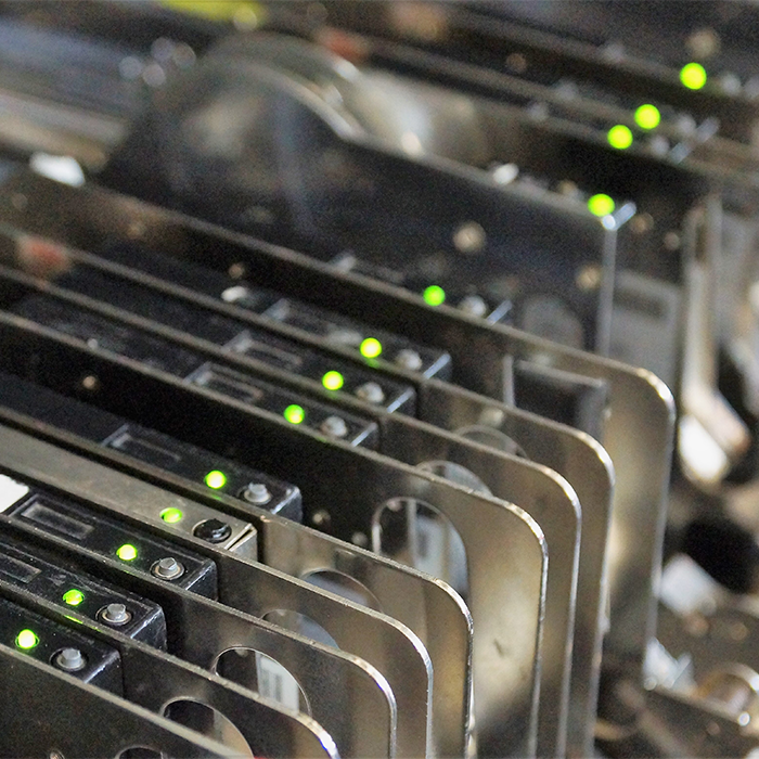
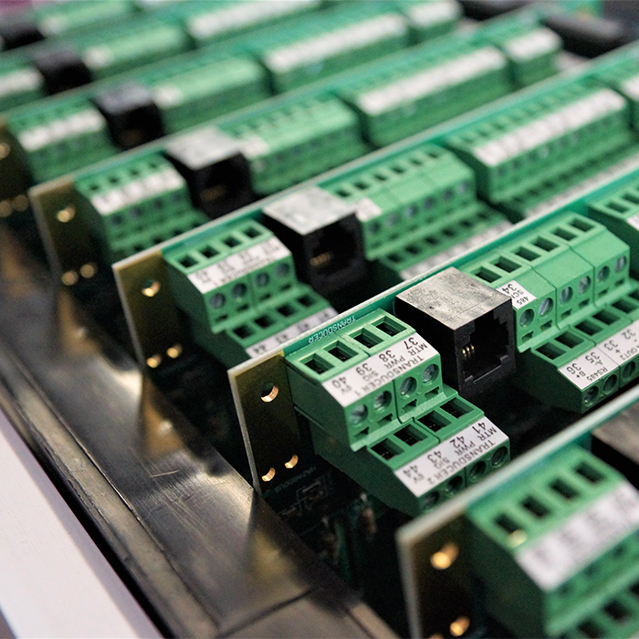

Through-Hole Assembly
What is Through-Hole Assembly?
Through-hole assembly is a soldering technique employed in PCB manufacturing, primarily dedicated to securing electronic components with leads that traverse through holes in the PCB. This method ensures a strong mechanical and electrical connection, making it ideal for components requiring enhanced stability and durability.
Through-hole assembly finds its niche in a variety of applications, including automotive electronics, industrial controls, medical devices, and aerospace systems. In the ever-evolving landscape of PCB manufacturing, Through-Hole Assembly remains a steadfast technique, embodying the essence of reliability and strength. From classic applications to cutting-edge innovations, Through-Hole Assembly continues to shape the backbone of electronic connectivity, ensuring that each connection is a testament to precision and durability.
Click here to view More Details

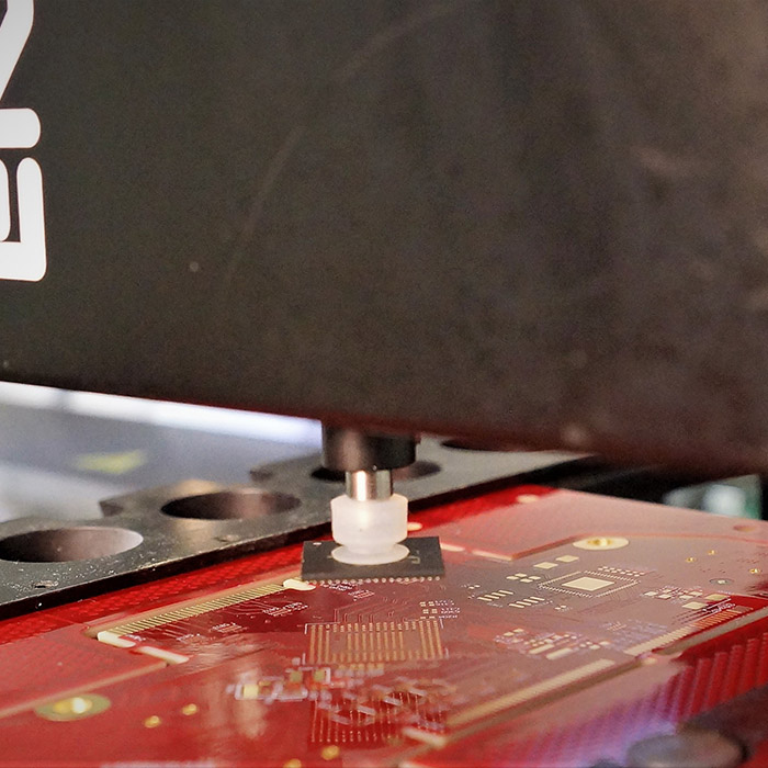
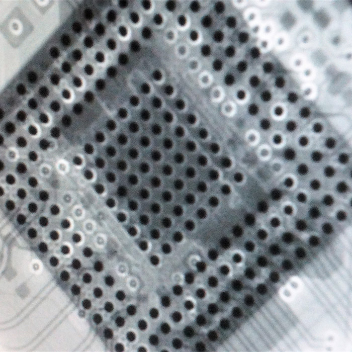
X-Ray Inspection
What is X-Ray Inspection?
In the intricate world of printed circuit boards (PCBs), ensuring the quality and integrity of components is paramount. The X-Ray technique helps to provide unparalleled insight into the hidden realms of electronic connections. X-Ray provides an answer where you cannot optically see the solder connections, and gives PCB Manufacturers a method to examine the internal structures of PCBs without compromising their integrity.
Click here to view More Details
Downloads Centre
Access technical datasheets, product manuals, compliance certificates, safety guidelines, and more all in one centralised location.